I don't get transistors

I’ve been given a physics class to teach in HS, and some of them aren’t very math oriented, so I’ve been trying to show how some practical things work, like car engines, refrigerators, CD players, speakers, microphones, etc. I’ve now tried to add transistors.

I just don’t understand why putting a current flow into the n type end and out the depletion zone is so much better than putting the voltage drop through the whole thing with the bigger battery.

Here’s my logic now that I’ve had a think about it:
The tiny current through the n type left end and out the depletion region frees up holes in that region, which lets the bigger current get through that region and start a full circuit. How does that sound?

Here’s what I don’t understand:
The voice says that the current doesn’t keep on going in the smaller circuit, but the animated electrons keep flowing. Which is right? Furthermore, if the whole bigger circuit doesn’t need the smaller circuit to be on, then I can’t turn this off, so it seems that it would need the smaller circuit to stay on. But why would turning off the smaller circuit turn it off once it’s going? Or is there another way we turn off the bigger circuit?

Don’t feel bad. I’m an EE, have taken two semiconductor physics courses, and I still don’t have a solid understand of how a BJT works. I guess I just have a hard time forming an intuition of electron and hole flow through semiconductor materials.

Since taking those classes, I haven’t put any additional effort into trying to understand the inner-workings of the BJT. I much prefer to learn about the BJT from the “black box” perspective, i.e. I look at it as a three-terminal device where the base current magically controls the collector current in the active region. There’s also the cut-off region and saturation region. Throw in a few simple equations, and you’ll have it mastered. :slight_smile:

Upon further reflection, I now realize my post is not much help to you; you’re teaching physics, not EE. I apologize for that.

In my opinion EE and semiconductor physics books do a very poor job of teaching how transistors work. I wish I knew of a good reference that does a decent job of explaining it. :frowning:

The video clip does not really explain anything in depth, but it at least addresses your questions:

The point is that the small current is amplified, and without it no current flows at all “through the whole thing”.

The voice says that without the smaller circuit you essentially have two diodes back to back, so no current will flow in that case. In that sense, the small current really is switching the transistor “off” and “on”.

The way I learnt about transistors was to first learn about triodes. Triodes are more intuitive and once you get that, you’ll get an understanding of transistors too.

If you are planning to teach about transistors, you had better learn how they work.

Statements like the quote are common but wholly wrong.

A transistor is a voltage-operated device, responding to the voltage between base and emitter. The current that flows into the base is a result of that voltage and is just an annoyance; it does not make the transistor work. So transistors are designed to keep it as low as possible.

This Wikipedia gives some more information; in particular look at the Ebers-Moll model:

Not wishing to be discouraging but you do need a grasp of Ebers-Moll. You won’t need the math beyond that.

I totally agree with this. I learned about triodes at a time (around 1955) that transistors were still lab curiosities, but had not entered consumer products. Briefly, a triode consists of a heated cathode at ground, an anode (called a plate) usually at around 100-200 volts and a grid (a metal lattice) in between. The cathode boils off electrons which are attracted to the plate going through the grid. If there is no voltage on the grid, the electrons are not impeded. But even a few volts negative on the grid will repel the electrons to the extent that no current flows. And a few volts positive will encourage the flow. The result is that the current flow is determined by a few volts change in the grid. And if that current goes through a resistor, then a small change in the grid voltage will result in a large change in the voltage across that resistor. Note the change is in the opposite direction. The amount by which the voltage is amplified is called the gain. Typically triodes had gains under 100. But multigrid tubes could have gains of a 1000 or more.

Do you have the option to teach MOS transistors instead of BJTs? They are much easier IMHO to understand, especially if you are mainly concerned about application to digital circuits (where they are basically voltage controlled switches). You can get past device physics much more quickly, then move on into combining them into logic gates (and, or, inverters) and memory elements (flip-flops, memory). They are the basic building block of the digital world.

ETA: Mathematically a MOSFET is very similar to a triode but is more relevant to modern electronics.

A triode is a voltage-controlled device, like a MOSFET, unlike a BJT, which is current-controlled.
Voltage-controlled devices are much easier to understand.

I apologize for (and please correct) any misleading or false statements. Of course the base current is not magically amplified, and without the base-emitter bias voltage the transistor will not conduct at all (or not much).

The specific question was

and my answer was that such a transistor can be used as an amplifier, and that would be one possible reason to hook it up in this common collector configuration where some current flows from the base to the emitter. (More detailed analysis is required to sketch an actual linear amplifier.)

Those are the stripy things, right?

Actually, a BJT (bipolar junction transistor) is considered a current controlled device. The input (base) current is that of a forward biased diode - once you bias it with enough voltage to get the current flowing, any increases in base current require very small increases in base voltage. In most cases you assume the base-emitter voltage is constant and you design your biasing circuit to provide the desired base current given that fixed base-emitter voltage. Designing a biasing circuit to provide a defined base-emitter voltage is generally bad design practice.

This assumes you are building an amplifier. If you are building a digital logic gate (like TTL logic) then the considerations are different since you are not holding the transistor in forward active mode.

could be right, but I don’t like it. It’s been a long time, but here’s how I remember it was:

A large (majority carrier, electron) current flows out of the Emitter (N on an NPN transistor). Some of this current dribbles out the base: the rest of it is swept out (collected by) the collector. Electron flow opposite to “conventional current”.

You are trying to get base current: your external circuit is set up get base current through the Emitter-Base diode. It’s just that when you run current through the base region, most of the f’ing electrons gets swept out and collected by the collector. So it’s actually the /collector/ current that’s leakage: all of your emitter current is leaking out the collector.

Perhaps I could say that the BE junction is a slingshot: the base keeps cocking the gun and the emitter keeps firing bullets, but most of them are overshooting and landing in the collector.

Posted before finished thinking:

If you wanted to build a model, you could have balls rolling down out of the emitter. The base is tilting the platform: you could have a bias circuit where balls coming out the base connection land on a balance that pushes the base up: if no current flows out the base, the base circuit pulls the base down until some ball do roll down the base connector.

But most of the balls rolling out of the emitter miss: they roll past the hole and are collected by the collector. /NOTHING COMES OUT THE COLLECTOR UNLESS THE BASE EMITTER BIAS CAUSES BALLS TO ROLL/

If you wanted to make it more detailed, you could add the fan that sweeps the balls away from the base lead, towards the collector. If you wanted to be more technical, you could use charged plastic balls, with an electric field to sweep them towards the collector. In any case: nothing collected by the collector unless it’s coming out the emitter: nothing coming out the emitter unless the base is pulled.

I found this page with diagrams and equations describing an “ideal” (and, further on, non-ideal) bipolar junction transistor. The diagrams are a little crude, but compared to the video at least you can see all the modes of operation of the transistor, as well as the electron and hole flow in the forward-active region.

Sometimes, I’ll read a Dope thread and realize that every word is in English and that I understand the meaning of every word, but the whole things makes absolutely no sense to me.

This is one of those threads.

That is what several EE professors told me. That description is common in many textbooks plus the 1st paragraph of the cited Wikipedia article: “The basic function of a BJT is to amplify current”. In fact the common figure of merit Beta means collector current divided by base current, which is the BJT’s gain.

So I don’t understand the statement that a BJT transistor (the OP question) is a voltage-controlled device. The OP was asking specifically about BJT transistors, not FETs.

Re Ebers-Moll, this was a question about a high school class. At the high school level I’d recommend not getting bogged down in gate physics, academic white papers, electronic vs hole flow, etc. It would likely be more practical to illustrate and discuss real-world examples which show transistor operational characteristics and behavior.

E.g, why do modern CPUs get so hot when switching speed increases? A main reason is they’re spending more time in the active region, not saturation or cutoff. This could be illustrated with a transistor characteristic curve: https://www.electronics-tutorials.ws/transistor/tran37.gif

A modern CPU uses FETs not BJTs, but the same principle applies: in cutoff no current flows, so there’s little power dissipation. In saturation the transistor approximates a conductor having little resistance, so likewise little power dissipation. As it switches ever faster, it spends more time in the transition or ohmic range where it is dissipating power.

This also explains why a high-power semiconductor linear amplifier is difficult (and expensive) to construct even today. By contrast a high-power semiconductor relay can handle very high power because it’s either on or off.

CPUs which contain billions of transistors do not tolerate heat well, as seen by the constant focus of computer hobbyists on “never exceed” CPU temperatures, which are quite low.

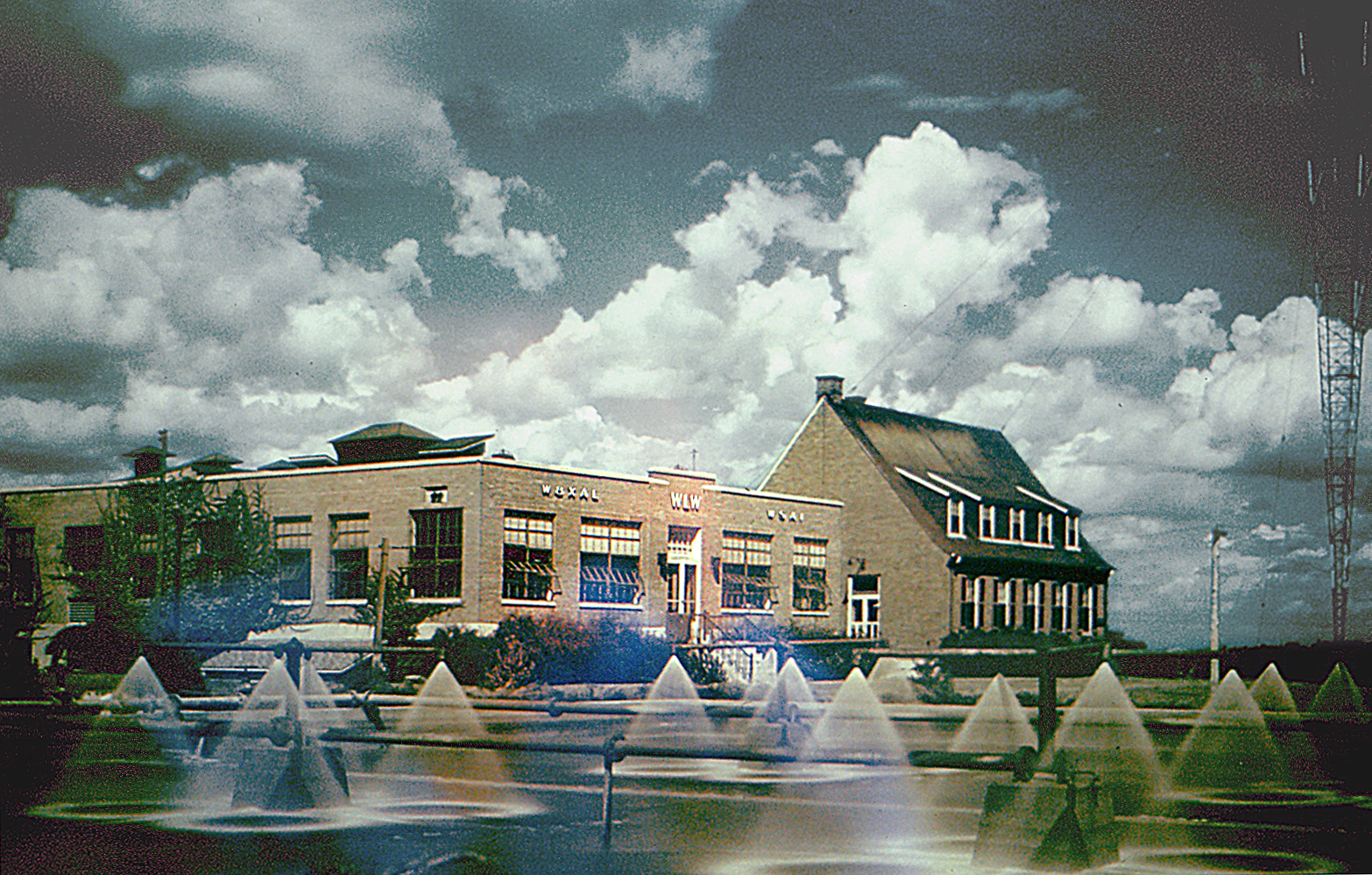
By comparison a vacuum-tube linear amplifier can handle tremendous power, partially because it can tolerate heat. This photo shows two of 20 final amplifier tubes from WLW which before WWII handled 100,000 peak watts per tube, or two megawatts peak envelope power total. The base is a water cooling jacket which was piped to a cooling pond.


Today high power solid state broadcast linear amplifiers still cannot manage high power per device so they digitally split the signal across 60 or so RF modules then combine the output. To equal the WWII-era WLW output would require about 600 solid-state transmitter modules.

The question, “Is a BJT a current-controlled device or a voltage-controlled device?” has lead to many debates.

The answer? It is a current-controlled device or a voltage-controlled device depending on how you look at it.

When you peer inside the transistor and study the physics of how it works, you learn the voltage between the base and the emitter controls the collector current.

So… with this information you grab a regulated power supply and apply 0.7 V between the base and emitter of a NPN transistor. The resulting base current is 1 mA and the collector current is 100 mA. (I am leaving out the other circuit elements here, obviously.) Time to get out the beers, right? Nope. Because after a couple minutes the transistor will smoke and fail. Why? Because a silicon PN junction has a negative temperature coefficient, and sticking a stiff, external voltage source across it will lead to thermal runaway. (In this case, the base-emitter junction.) This is also true for silicon diodes.

Due to its negative temperature coefficient, a silicon PN junction becomes very unhappy if you stick a stiff voltage across it, but becomes very happy if you inject a stiff current through it. Unlike the former, the latter won’t lead to thermal runaway.

So… when we use a BJT, we must inject a “controlled” current into the base. To do this, you can use a true constant current source or (more commonly) a pseudo constant current source. A pseudo constant current source is simply a resistor in series with voltage source. (Even then, you have to be careful. If the pseudo constant current source starts to look more like a pseudo constant voltage source due to the value of the series resistor being too low, thermal runaway will still occur.)

So that’s the primary reason we talk about controlling the base current and not the base voltage: because you need to inject a controlled current into the base when using the BJT in a circuit else thermal runaway could occur. Another reason is because there’s a simple, linear relationship between the base current and collector current when it’s in the active mode. By contrast, the relationship between the base-emitter voltage and collector current is an uglier exponential equation.

I’m starting to think this school starts each semester by having you pull a class out of a hat. Surprise! It’s physics time!

If you don’t expect to build on the actual physics of transistors in the class, there is a nice analogy that illustrates “how it works” for electrical circuits including transistors - the hydraulic analogy.

As with all analogies, it breaks down when attempting to explain all of the properties of transistors, but it is a great way to show something no one can “see” into something that a lot of people can relate to things they’ve seen. It is a great way to get across “when you increase the voltage (pressure) here, the Current (flow) there does that”. Just don’t try to explain holes/electrons, bandgaps, or fermi levels.

Googling water transistor analogy and hydraulic transistor analogy provides a wealth of information, including some YouTube videos. And there is always the potential to build a hands on demonstration if you have the inclination.